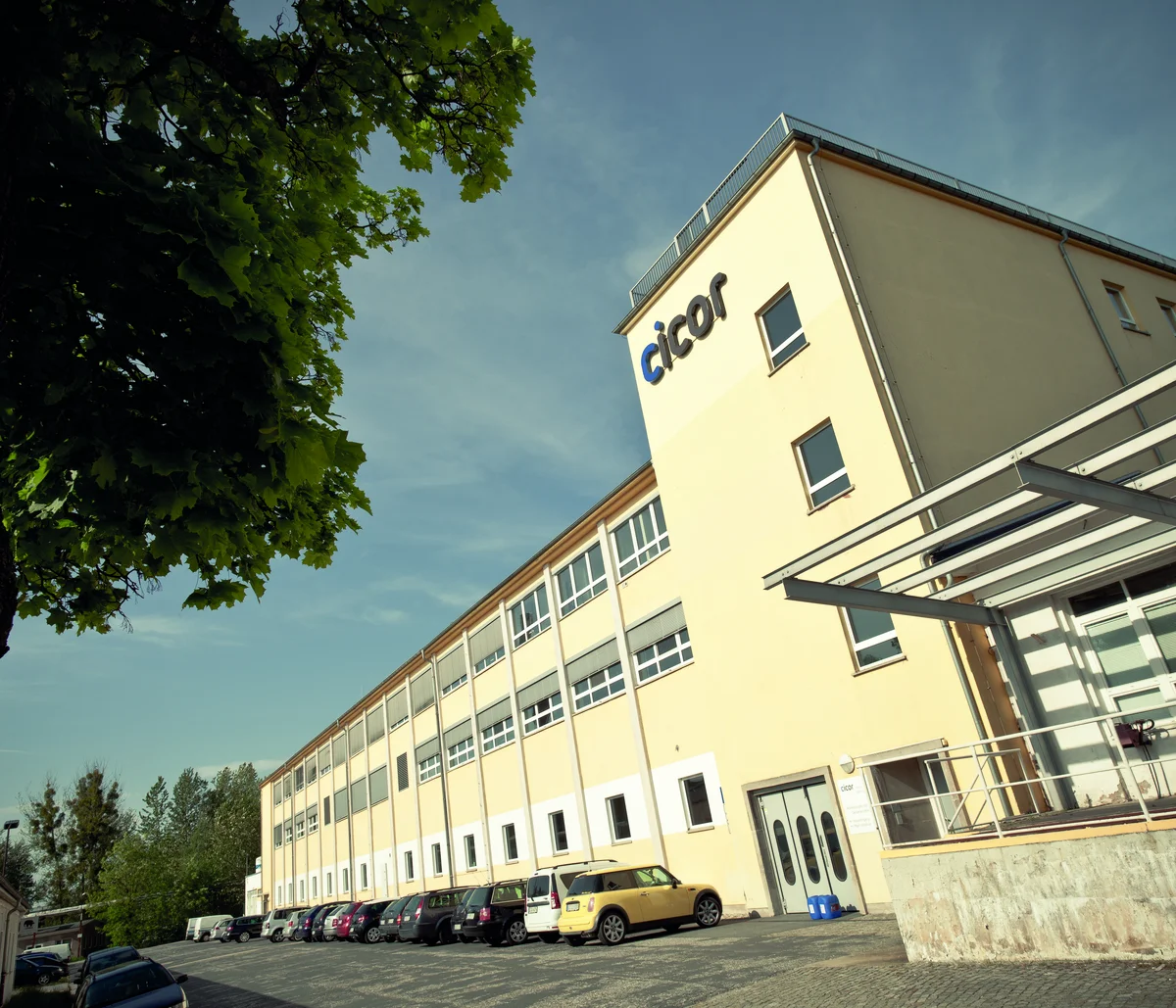
Radeberg, Germany
Your specialist for microelectronics and thick-film substrates
The Radeberg location specialises in the production of complex, high-reliability ceramic substrates using thick-film technology.
Microelectronic assemblies on ceramic or printed circuit board substrates or in hermetic hybrid housings are also assembled on site. A wide array of electronics packing technology (EPT) processes are available for this purpose.
- Founded in 1991, the Radeberg location offers a range of services, including development support, prototyping, product certification and serial production.
- EPT in Radeberg comprises various processes and technological options for manufacturing electronic assemblies under cleanroom conditions. For example:
- Thick-film technology for the production of ceramic-based electrical circuit boards
- Chip bonding (gluing, vacuum soldering, sintering)
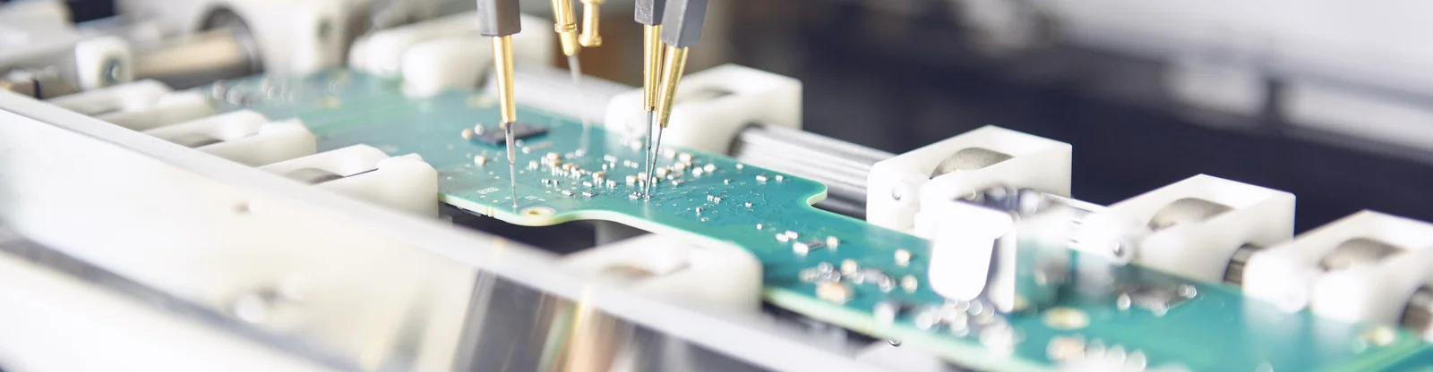
- Wire bonding (Al bonding, Au bonding, ball-wedge/wedge-wedge, thick wire/thin wire)
- SMD assembly with AOI and X-ray inspection
- Encapsulation (hermetic sealing by welding the lid onto the housing, non-hermetic sealing by means of globtop, moulding, gluing caps)
- Laser processing (labelling, cutting, resistor trimming)
- Electrical test (ICT, function test)
- Electrical test benches are developed and built in-house to guarantee reliable electrical testing to customer specifications.
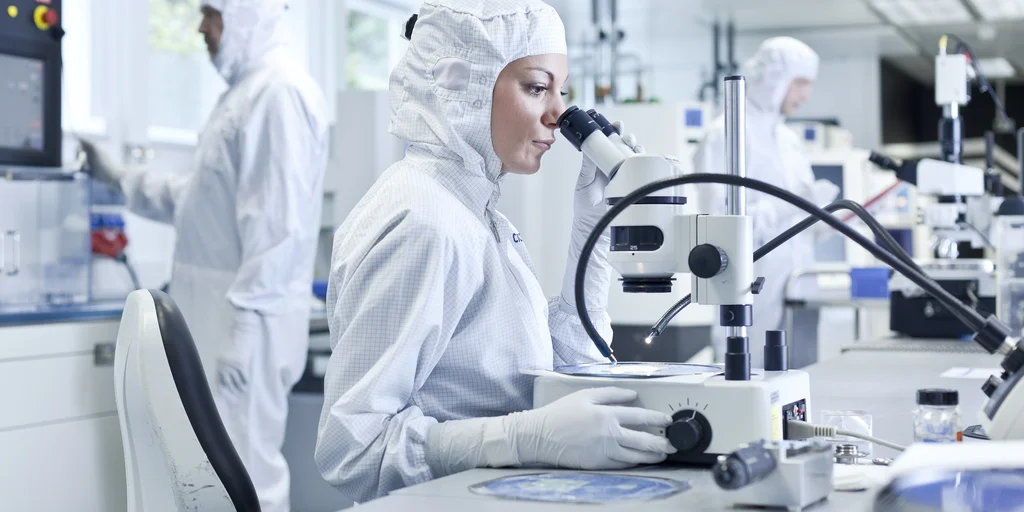
- The production facilities comprise 1,300 m² of cleanroom space with classifications ranging from ISO 7 (class 10000) to ISO 5 (class 100) for production compliant with high cleanliness requirements.
- The core sectors are aerospace, defence, medical technology and sophisticated industrial applications.
- The location is certified to industry standards and has ISO 14001, ISO 9001 and ISO 13485 certification. The location is also certified to EN 9100 Aerospace and KTA 1401 Nuclear Power Plants.
Expertise and Services
Microelectronics assembly (EPT), Assembly / Packaging
In addition to thick-film technology, the Radeberg location also offers a wide range of high-precision production technologies for the assembly of microelectronic components. The focus is on the processing of various substrates (such as printed circuit boards, flex, ceramic and lead frames), as well as the assembly of hybrid electronics in metal and ceramic enclosures.
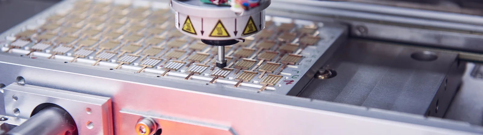
For the assembly of bare chips (chip-on-board COB), modern connection methods such as bonding, Ag-sintering and flux-free vacuum soldering are used, in order to satisfy the highest standards in terms of connection quality and cleanliness. Various wire-bonding processes, materials and wire thicknesses are then available for electrically contacting the chips. Many different component types and sizes are processed in SMT production, ranging from the smallest chip components of size 01005 to large area array components (e.g. BGAs). Flip-chip assembly with direct contacting of chips using reflow soldering is also possible.
To guarantee the highest quality standards, automated inspections of the printed solder paste and the finished soldered assembly are performed using AOI. X-ray inspection is also used for non-visible soldered joints. Electrical tests to specific customer specifications on specially developed test benches round off the comprehensive quality testing programme.
In subsequent process steps, the manufactured assemblies are separated as required or processed for further integration, e.g. in hermetically sealed housings.
The separation processes used include the laser separation and depaneling of printed circuit boards, as well as scribing/breaking for ceramic substrates, which are specially produced using thick-film technology.
To achieve hermetic encapsulation, the module, which is integrated and contacted in an enclosure, is finally hermetically sealed with a welded cover. Non-hermetic encapsulation processes such as globtopping, potting or applying caps are available as an alternative, to protect sensitive assemblies or parts thereof.
The labelling of assemblies and products using laser marking or labels is standard practice at Cicor. This guarantees maximum traceability of all components.
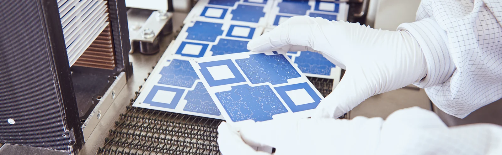
Thick-film Technology
The Radeberg location specialises in the processing of ceramic, steel and glass substrates in the field of thick-film technology. The core process for manufacturing circuit boards using thick-film technology is the time-tested screen printing process. This allows conductive and resistive pastes, as well as insulating pastes and glazes, to be processed and built up into complex multilayer circuit carriers. It permits minimum structure resolutions of as low as 80 µm (line width/space). The surfaces can then be finished with additional coating processes. The finished printed electrical resistors are calibrated with high precision by laser resistor trimming after baking and the substrates can also be electrically tested by means of a carrier board test.
Test Development / Test Method
To ensure the quality and reliability of the products, the Radeberg location offers a wide range of testing services. These include electrical tests such as functional tests and ICT, as well as flying probe tests for carrier board testing and the burn-in of functional assemblies. Further reliability tests such as thermal shock and humidity tests, temperature storage, vibration tests and acceleration tests are carried out as required to assess the quality and reliability of assemblies. Leak testing (coarse and fine leak) for verifying the tightness of welded hermetic housings are standard procedure at Cicor in Radeberg.
This broad range of technologies and test procedures enables the Cicor location in Radeberg to produce sophisticated microelectronic solutions for markets such as medical technology, industry, aerospace and defence.
Contact
Contact us
Cicor Microsystems GmbH
Heidestrasse 70
01454 Radeberg
Germany
Work with us
Do you value open communication and short official channels? Is it important to you to work in a financially stable company with a long tradition? Are you looking for a familiar working atmosphere and at the same time appreciate professional company processes? Do you want to be a personality for your employer and not just a number? Then we invite you to get to know us better.