Leiterplatten
Cicor entwickelt und produziert seit über 50 Jahren anspruchsvolle flexible, starr-flexible und starre Leiterplatten (PCBs) von der Idee, über Prototypen bis hin zur Grossserienproduktion. Dank der umfassenden Fachkompetenz im Bereich der Multilayer-Boards (MLBs) und High-Density-Interconnects (HDIs) entwickelt Cicor innovative und zuverlässige Lösungen für anspruchsvolle Anwendungen in der Medizintechnik, Luft-/Raumfahrt und Verteidigung, Industriemärkten.
Dünne Materialien sowie Leiter- und Abstandsbreiten bis 25 μm ermöglichen eine weitere Miniaturisierung und fortschrittliche Ultra-HDI-Lösungen. Die neu eingeführte DenciTec®-Technologie eröffnet dafür vollkommen neue Möglichkeiten. Durch die Kombination von PCB-Verfahren und der Dünnschichttechnologie lassen sich innovative Schaltungen herstellen.
Flexible PCB
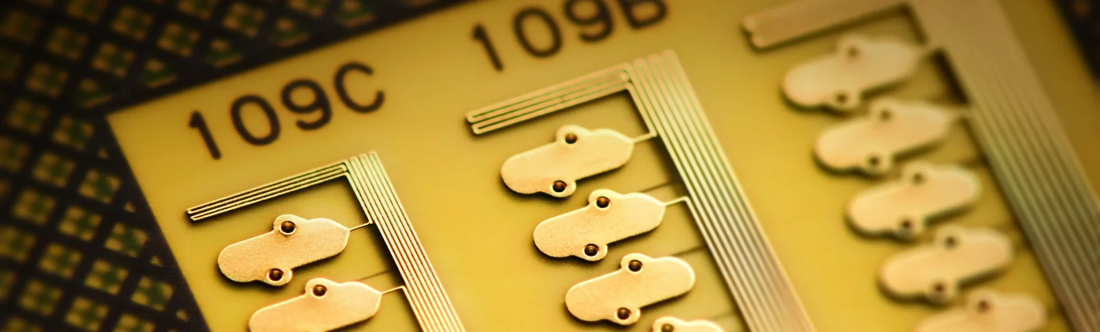
Flexible printed circuit boards (FPCs) are offering the highest level of 3D miniaturisation. Very low bending radii in combination with ultra-HDI are enabling our customers to build increasingly smaller and highly integrated devices. This technology is an enabler of small wearable devices as well it provides high signal integrity.
Cicor has been a market leader in this field for many years and is manufacturing flex circuits with a layer-count of 1 to 8. We are working with polyimide foils as thin as 12.5 µm and adhesive bond plys starting at a thickness of 12.5 µm. Our state of the art equipment is enabling us to produce FPCs with high output, reliability and repeatability. Depending on the dielectric thickness, laser drilled blind vias can be as small as 30 µm in diameter, and can be filled with copper in the subsequent plating process.
Leading edge alignment methods are enabling us to achieve very small annular rings and soldermask registration even on extremely complicated multilayer FPC. As an option, also coverlayer foils can be used. All standard surface finishings can be deposited on the boards, providing our PCBs suitable for all assembly methods. High accuracy laser contour cutting is generating radii of 0 µm and is optimising the real estate utilisation and enabling our customers to achieve excellent 3D miniaturisation.
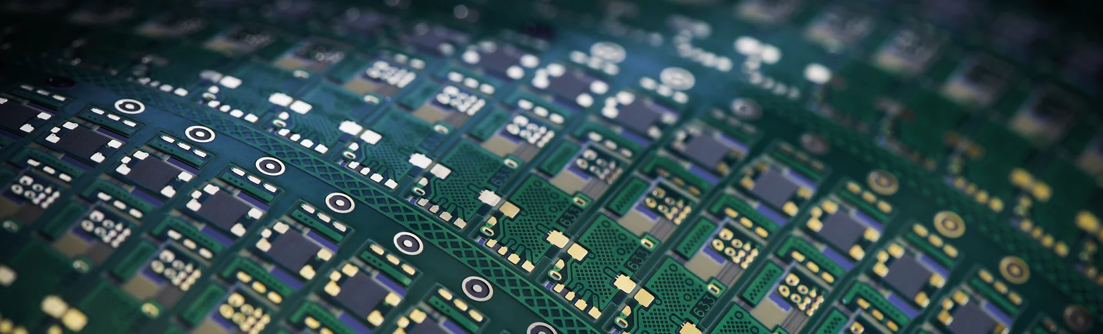
Rigid PCB
Rigid PCBs are available in many different varieties, differentiated by the number of layers, base materials used, construction methods, interconnection schemes as well as areas of use. Cicor is offering rigid PCBs with 1 to 12 layers with a clear focus on miniaturization in x, y and z axis.
Cicor is using (ultra-) thin high-end base materials, with CTE values in x and y down to below 8 ppmK-1, to minimize the CTE mismatch. The construction of the boards can either be parallel or sequential. Using state-of-the-art equipment, blind microvias as well as through holes can be drilled either mechanically or with laser. Subsequently, vias can be filled with copper to enable via stacking or staggering and via-in-pad designs. The utilization of these advanced design features is maximizing the design freedom and is one of the key factors for miniaturization.
All standard surface finishings can be deposited on the boards, providing our PCBs with finishings for all assembly methods used. High accuracy routing and laser machines are enabling us to cut outer contours with very tight alignment tolerances to the etched patterns. Additional features like edge plating, castellations, controlled impedances or (non-)plated cavities can be offered as well.
Rigid-flexible PCB
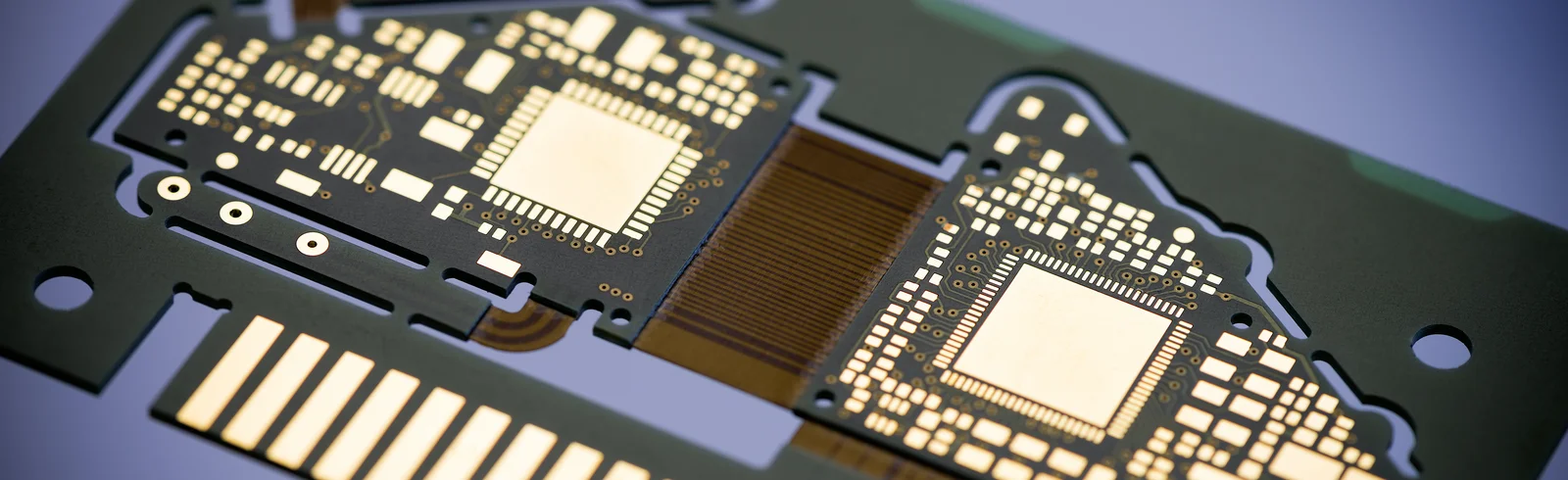
Combining the advantages of both, rigid and flexible PCBs in one circuit board offers several benefits:
- Replace rigid PCBs, connectors, cables or separate flexible circuit boards by integrating the connection of different parts in one single rigid-flex PCB
- Reduce the size of components and enabling 3-dimensional installation of assembled PCBs
- Increase reliability, especially in harsh environments including vibration, acceleration or deceleration, as connection is integrated in the circuitry
- Improved signal integrity
- Reduce logistic effort by combining several components within one single PCB
Cicor is offering a big variety of rigid-flex PCB constructions, using high end/quality base materials, like high TG/low CTE FR4, combined with polyimide foils and various adhesives. State of the art interconnection technologies like stacked or staggered vias and via-in-pad structures are used to drive miniaturization further down the road. A big portfolio of surface finishings is enabling Cicors customers to use all available assembly methods on boards produced by us.
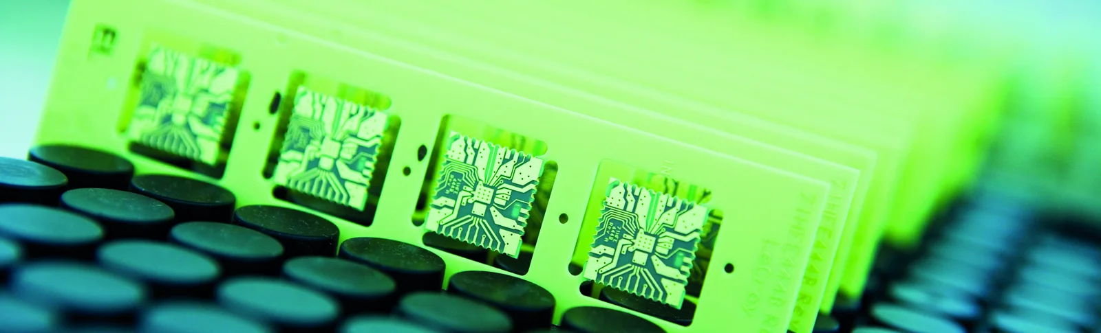
DenciTec®
Since 2016 Cicor has been offering DenciTec® PCBs. Highly sophisticated manufacturing technologies are enabling the production of very high-density circuits. State of the art equipments and new kinds of base-materials are making sure, that no concessions have to be made for Qality and design freedom..
DenciTec® makes further miniaturization possible:
- Line widths and spacings down to 25 µm (1 mil)
- Copper thicknesses of 20 µm (0.8 mil) +/- 5 µm on all layers
- Laser-via diameters of 30 µm (1.4 mil)
- Annular rings of 30 µm (1.2 mil) for the inner layers and 20 µm (0.8 mil) for the outer layers
- Copper-filled blind vias with the option of via stacking and vias-in-pads
- Even ultra-thin circuits are possible, using a 12.5 µm (0.5 mil) polyimide core material (4-layer flex circuits less than 120 µm (4.7 mil) thick)
- Maximum reliability
More freedom in design – greater functionality for equipment:
- Miniaturization: Significantly greater integration capabilities: More space for additional options such as energy supply (batteries, etc.)
- Higher packing density: More design options, no limitations in the use of design features
- Greater functionality: Smarter products with more functions
- Significantly lower manufacturing costs than with thin-film technology
Contact
Wir sind für Sie da
Unser PCB-Team steht Ihnen für alle Fragen zu Cicor und unseren Lösungen gerne zur Verfügung.